Principles
Create the future
Create the future
1. Client First
2. Wealthy character formation through acquiring the basic techniques
3. Create the new value for the society with innovation
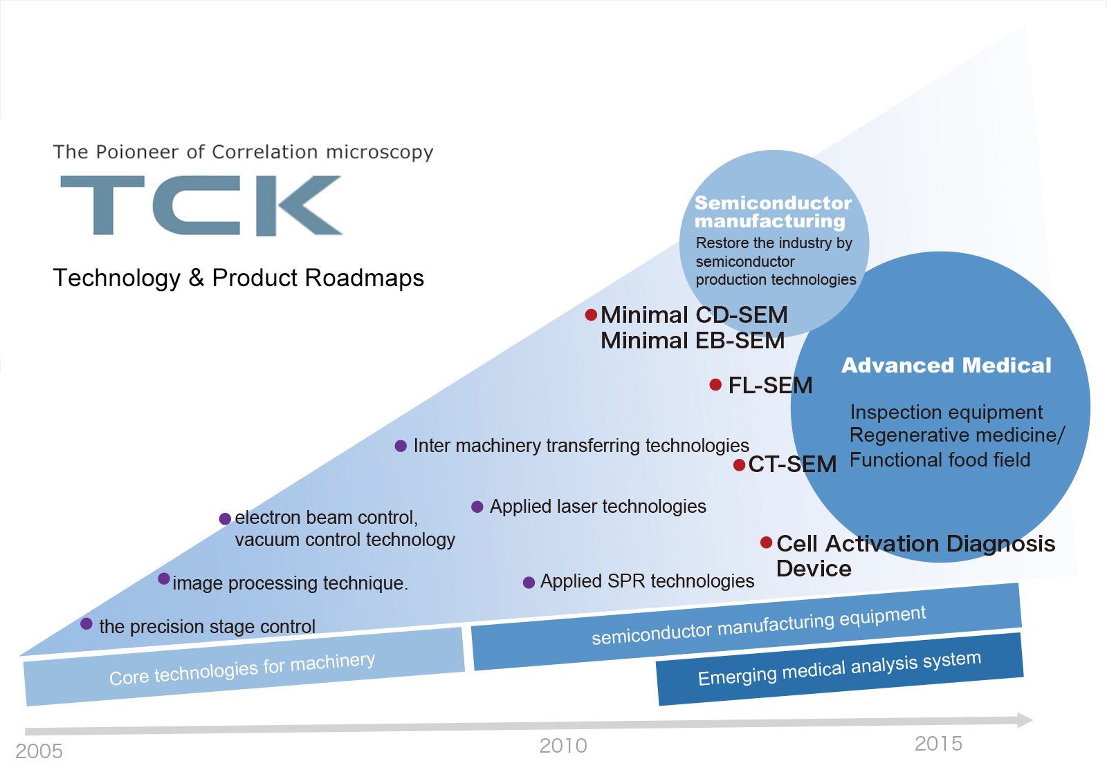
TCK inc. has developed and sold a lot of unique semiconductor related devices with the basic technology like the precision stage, vacuum control technology, electron beam control, and image processing technique etc. for the semiconductor industry, since its establishment in the year 2005. As the result, in the year 2014, a high resolution and ultrahigh vacuum SEM of smallest level in the world was developed and sold, and a lot of feedback was received from various fronts.
In the recent years, precision technology developed in the semiconductor field is applied, and new equipment development is in progress for state-of-the-art medical and material field.

| Company name | TCK inc. |
| Adress |
TCK Inc.
1-17, Futamatase, Higashi-ku, Fukuoka city, Fukuoka Pref., 812-0066, Japan TEL:+81-92-710-4100 FAX:+81-92-710-4200 |
| Establishment | Mar. 23, 2005 |
| CEO | Kouji Kosaka |
| Capital | 20,000,000yen (As of May, 2017) |
| Business Area |
|
| Corporate History |
|
| Major trading partners |
|
| for Environment | ||
|---|---|---|
| Clean booth: 1 set | Stone surface plate: 3 sets | Chiller |
| Ultrasonic cleaning machine | Carrying systems | Air slide: 2 set |
| for High precision measurement | ||
| Laser length measuring system: 1 set | Laser Doppler vibrometer: 1 set | Autocollimator: 1 set |
| Electric micrometer: 2 sets | Surface roughness tester | Micro fluxmeter |
| Micro precision flatness measure | Digital platform scale | Particle counter |
| Reference Standard in Measurement | ||
| Optical circuit & mirror: 3 | Optical flat: 1 set | Gauge block: 2 sets |
Parallel bar: 3 types |
||
| for Electronics | ||
| Oscilloscope :4 types | Logic analyzer | Digital multimeter |
| Others | ||
| Penning vacuum gage | Stereomicroscope | |