CD-SEM

  • Features
  • Specification
  • Application

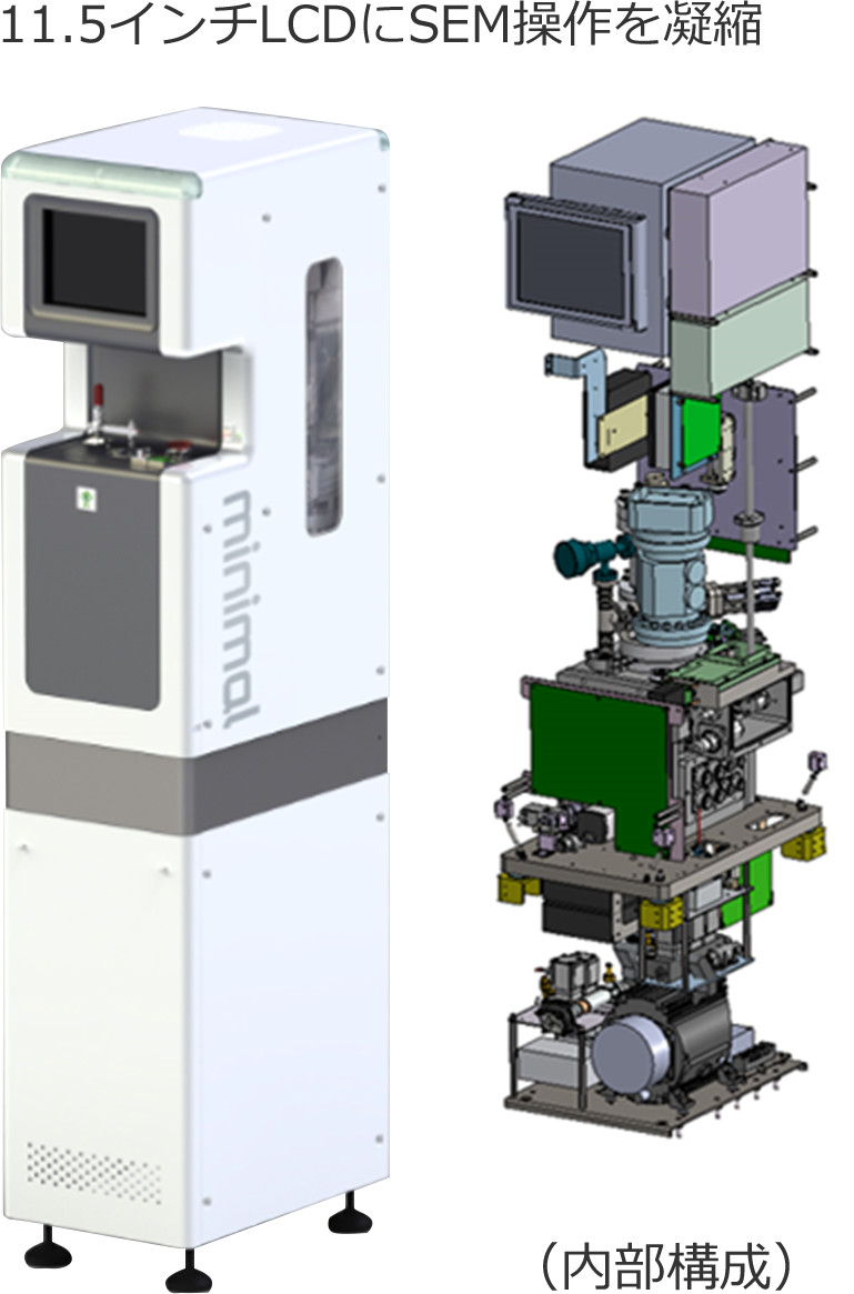
The SEM with size measurement functions based on the minimal standard.

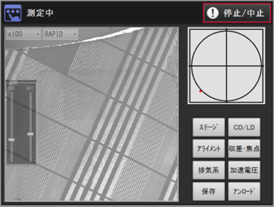
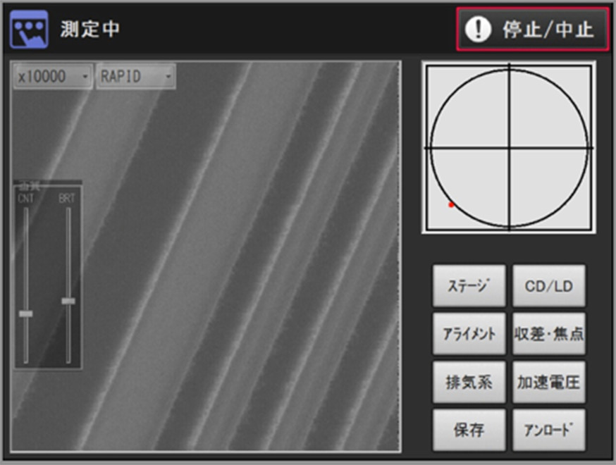
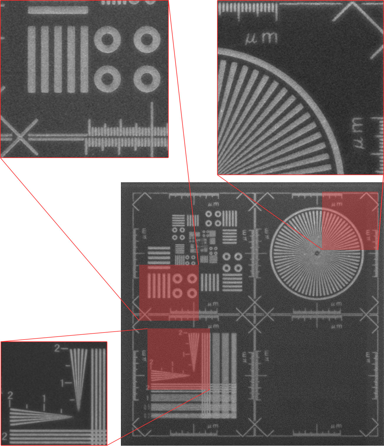
High resolution pattern measurement by using shotkey emission electron gun
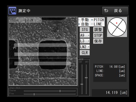
Position management of specimens by using auto precision stage
Clean measurement by using perfect dry vacuum system

Features

CD-SEM

Shotkey emission electron gun
Stable irradiation current and high resolution are accomplished.
Auto transfer system accordance with ultra-high vacuum
Because of auto transfer system, after specimens are set to stage, you can measure the specimens immediately by clicking the transfer button.
Perfect dry vacuum system
Diaphragm pump, turbo molecular pump and sputtering ion pump are installed for vacuum and exhaust system, clean-environmental measurement is realized.
Auto high-precision stage
Precision stage with four axis: X/Y/Z/R control is installed to chamber. Size measurement unit for each axis is installed, high precision positioning and size measurement are accomplished.
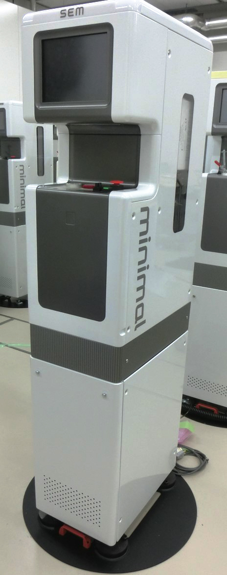
Compact body
Layout-free and portable SEM which can be set up for various situations.
Energy saving
Low energy consuming SEM which can be set up anywhere only with AC100V/4A power supply
Attachment integration
Multi-purpose instrument with various add-on: electron beam attachment for electron beam patterning, EDS attachment for element analysis and so on.

Minimal CD-SEM

Features

Minimal CD-SEM (Critical Dimension-Scanning Electron Microscope) is specialized for size measuring of wafer pattern among the electron microscope. The feature of this device is the movable size and weight (459mm in depth, 1440mm in height, 297mm in width, 120kg), and its realization of high resolution / ultra-high vacuum at factory lebel while being capable of operating in the domestic power supply in AC 100V.

width: 297mm depth: 450mm height: 1,440mm weight: 120kg power: AC100V/4A

Various way of network connection for realizing the portability

For the portability of this instrument, various way of network connection is installed such as PC connection by USB / LAN cable and IR internet connection by IR cloud internet.

Primary specification

Emitter ZrO/W
Accelerating voltage 1 ∼ 5kV (continuous variable)
Resolution 10nm
Magnification x50 ∼ x500,000
Sample size 0.5 inches
Stage components X-Y-Z-R Automatic
Stage precision Repeated positioning ± 0.1um
Detection of stage position Linear encoder 0.01um
Exhaust system Dry exhaust system
Sample conveying Fully automatic

Applications

Device evaluation

The size measurement of resist patterns by using minimal CD-SEM. Simple and easy measurement of fine device pattern is realized by using the software included.

100 10,000 CD

Screenshot of inclueded software. From left: x100, x10,000, processing screen

Device fabrication

Patterning of resist of silicon wafer by using the electron beam (EB) attachment.

Photoresist used: ZEP520A (Xeon)